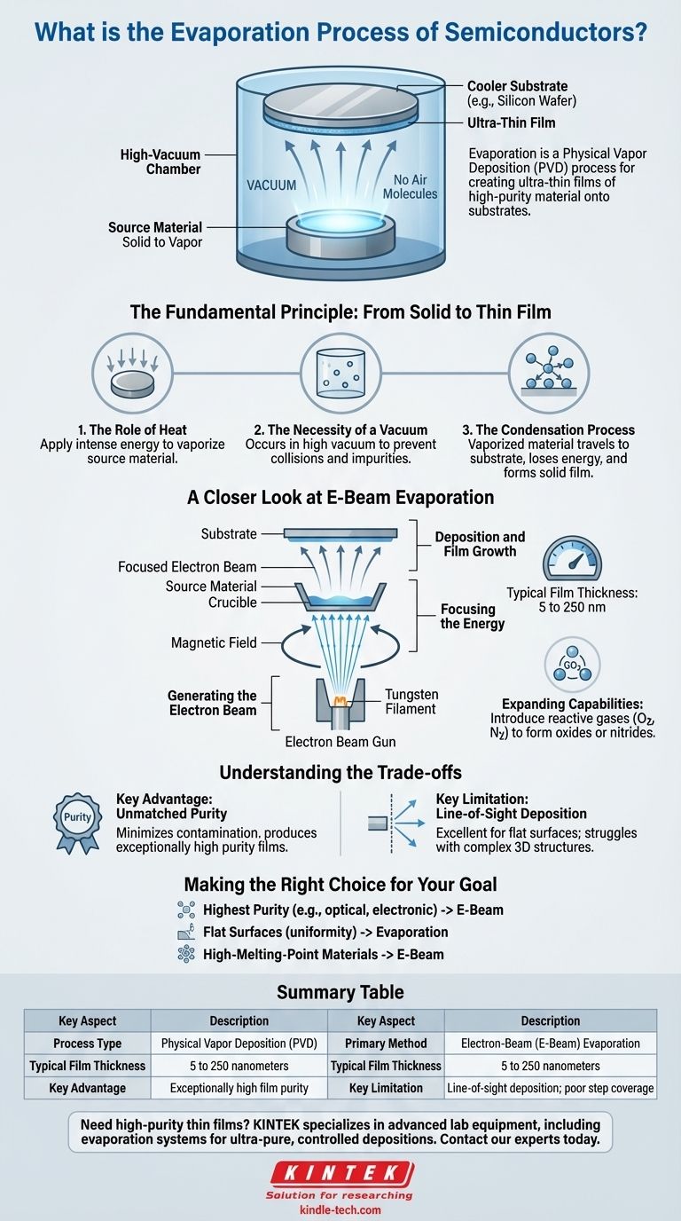
半導体の文脈において、蒸着(エバポレーション)とは、シリコンウェハーなどの基板上に材料の超薄膜を作成するために使用される物理気相成長(PVD)プロセスです。これは、チャンバー内の原料材料を加熱してガス化させるプロセスを含みます。これらの気化した原子は真空を通過し、より冷たい基板上に凝縮して、固体の高純度膜を形成します。
蒸着の核心原理は、真空中で熱エネルギーを利用して固体材料を蒸気に変換し、それがターゲット表面上に精密に制御された薄層として再固化することです。この手法は、マイクロプロセッサや集積回路に見られる複雑な構造を構築する上で不可欠です。
基本原理:固体から薄膜へ
蒸着は、原子レベルの構築のために設計された3段階のプロセスです。各ステップは、最終膜の品質と完全性を確保するために極めて重要です。
熱の役割
プロセスは、小さなペレットやインゴットの形で原料材料に強いエネルギーを印加することから始まります。目標は、材料の温度を蒸発点まで上昇させ、蒸発(または昇華、固体から直接気体へ移行)させることです。
真空の必要性
このプロセス全体は高真空環境下で行われます。真空は、蒸発した原子と衝突し、原子を偏向させたり、膜に不純物を導入したりする可能性のある空気やその他のガス分子を除去するために不可欠です。
凝縮プロセス
遮るもののない経路を経て、蒸発した材料は原料源の真上に戦略的に配置された基板に直接移動します。冷たい基板表面に接触すると、原子は熱エネルギーを失い、凝縮して表面に結合し、目的の薄膜を徐々に構築します。
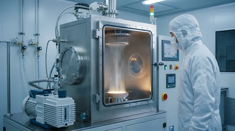
電子ビーム蒸着の詳説
いくつかの加熱方法がありますが、電子ビーム(E-beam)蒸着は、その精度と幅広い材料を処理できる能力から、半導体業界で主要な技術となっています。
電子ビームの生成
プロセスは、高温に加熱されて電子の流れを放出するタングステンフィラメントから始まります。これらの電子は、高電圧フィールドによって加速されます。
エネルギーの集束
強力な磁場が使用され、これらの高エネルギー電子を狭いビームに誘導し、集束させます。このビームは、るつぼと呼ばれる容器に保持された原料材料に正確に向けられます。
成膜と膜の成長
電子ビームからの強烈なエネルギーが原料材料を溶融し、次に蒸発させます。結果として生じた蒸気は上方に流れ、基板上に堆積し、非常に高純度の膜を作成します。最終的なコーティングの厚さは厳密に制御され、通常は5から250ナノメートルの範囲です。
反応性ガスの導入による能力の拡大
E-beamプロセスは、化合物を生成するように適応させることができます。成膜中に酸素や窒素などの反応性ガスをチャンバーに導入することにより、ウェハー上に金属酸化物や窒化物などの非金属膜を形成することが可能です。
トレードオフの理解
蒸着は強力な技術ですが、他のすべての工学プロセスと同様に、特定の用途への適合性を決定する特定の利点と制限があります。
主な利点:比類のない純度
E-beam蒸着の主な利点は、極めて高い純度の膜を生成できることです。電子ビームによって直接加熱されるのは原料材料のみであるため、加熱装置やるつぼからの汚染は最小限に抑えられます。
主な制限:直線的な成膜(Line-of-Sight Deposition)
蒸着は方向性のある、直線的なプロセスです。原子は原料源から基板へ直線的に移動します。これは平坦な表面のコーティングには優れていますが、アンダーカットやトレンチのある複雑な三次元構造を均一にコーティングするのは困難です。
目標に応じた適切な選択
適切な成膜方法の選択は、膜と製造されるデバイスの特定の要件に完全に依存します。
- 最高の膜純度を達成することに主な焦点を当てる場合:特にデリケートな光学層や電子層の場合、E-beam蒸着がしばしば優れた選択肢となります。
- 比較的平坦な表面に膜を堆積する場合:蒸着は、単純な形状に対して優れた均一性と制御性を提供します。
- 高融点の金属や特定の誘電体を堆積する必要がある場合:電子ビームの集束されたエネルギーは、これらの堅牢な材料を効果的に蒸発させることができる数少ない方法の1つです。
蒸着は、現代のマイクロエレクトロニクスの複雑な世界を構築するために必要な精密な層形成を可能にする基礎技術です。
要約表:
| 主要な側面 | 説明 |
|---|---|
| プロセスタイプ | 物理気相成長(PVD) |
| 主要な手法 | 電子ビーム(E-Beam)蒸着 |
| 典型的な膜厚 | 5から250ナノメートル |
| 主な利点 | 極めて高い膜純度 |
| 主な制限 | 直線的な成膜。ステップカバレッジが不十分 |
半導体の研究開発または生産のために高純度薄膜が必要ですか?
KINTEKは、半導体製造の精密な要求を満たすための蒸着システムを含む高度なラボ装置を専門としています。当社のソリューションは、次世代のマイクロプロセッサと集積回路の構築に不可欠な超高純度で制御された成膜を実現するのに役立ちます。
当社の専門家に今すぐお問い合わせいただき、当社の蒸着技術がお客様のラボの能力をどのように向上させられるかをご相談ください。
ビジュアルガイド
関連製品
- 蒸着用電子ビーム蒸着コーティング金めっきタングステンモリブデンるつぼ
- 高温用途向け電子ビーム蒸着コーティングタングステンるつぼおよびモリブデンるつぼ
- 電子ビーム蒸着コーティング 無酸素銅るつぼおよび蒸着用ボート
- 半球底タングステンモリブデン蒸着用ボート
- 電子ビーム蒸着用高純度純グラファイトるつぼ


