最も基本的なレベルでは、薄膜の役割は、材料の微細な層を表面に適用し、その表面に本来持っていなかった全く新しい特性を与えることです。これらの設計された層は、現代技術の目に見えない基盤であり、眼鏡の反射防止コーティングからスマートフォン内部の複雑な回路、太陽電池の効率に至るまで、あらゆるものを可能にしています。
薄膜の核となる機能は、単に表面をコーティングすることではなく、その表面が光、電気、熱、または物理的環境とどのように相互作用するかを正確に設計することです。この原子スケールでの制御こそが、数え切れないほどの現代デバイスの性能と機能性を可能にしているのです。
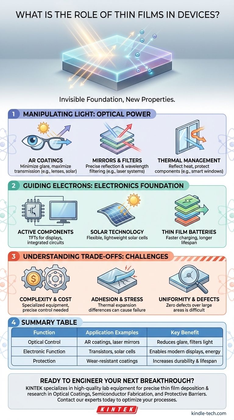
光の操作:薄膜の光学的能力
薄膜技術の多くは、光の流れを制御することに捧げられています。特定の材料を1層または複数層堆積させることにより、どの波長が反射、透過、または吸収されるかを正確に決定できます。
透過率と効率の向上
反射防止(AR)コーティングは主要な例です。これらは、カメラレンズや眼鏡から太陽電池や電子ディスプレイに至るまで、あらゆるものに使用されています。
これらのコーティングは、自然な反射を低減するように精密に設計された層であり、グレアを最小限に抑え、表面を通過する光の量を最大化します。これは、太陽電池の効率やディスプレイの鮮明度を直接向上させます。
反射の制御とフィルタリング
薄膜は、高度に専門化されたミラーやフィルターを作成するために不可欠です。例えば、高出力レーザーシステムでは、特定の波長に対してほぼ100%反射するミラーを作成するために、交互に積層された薄膜であるブラッグ反射層が使用されます。
同様に、異なる材料を層状に重ねることで、エンジニアは非常に狭いバンドの光を遮断するノッチフィルターや、可視光を通しながら赤外線熱を反射する建築用ガラスのコーティングを作成できます。
熱エネルギーの管理
薄膜は熱管理においても重要な役割を果たします。白熱電球の内部には、熱をフィラメントに戻して明るさと効率を高めるために、赤外線反射コーティングが堆積されています。
データストレージデバイスや窓ガラスでは、特定の薄膜が熱バリアとして機能し、敏感なコンポーネントを温度の急上昇から保護したり、建物への熱の侵入を防いだりします。
電子の流れを導く:現代エレクトロニクスの基盤
半導体産業全体は、薄膜の精密な堆積の上に成り立っています。集積回路内部の微細なトランジスタや経路は、導電性、絶縁性、半導性のフィルムを層状に重ねることによって構築されます。
能動部品の構築
薄膜トランジスタ(TFT)は、LCDやOLEDスクリーンを含む現代のフラットパネルディスプレイのバックボーンです。ディスプレイの各ピクセルは、堆積された薄膜で作られた独自の小さなトランジスタによって制御されています。
この同じ原理により、柔軟性、軽量化、エネルギー効率の向上といった利点を提供する薄膜太陽電池やバッテリーの作成が可能になります。
新エネルギー技術の実現
薄膜技術は、再生可能エネルギーと蓄電の進歩を推進しています。薄膜太陽電池は柔軟な基板上に製造できるため、従来のシリコンパネルが実用的でない新しい用途が開かれます。
同様に、薄膜バッテリーは、民生用電子機器から電気自動車に至るまですべてのクリティカルな要素である、より速い充電速度と長寿命を約束します。
トレードオフの理解
薄膜技術は非常に強力ですが、導入には課題がないわけではありません。これらの層を堆積させるプロセスは、材料科学における高度に専門化された分野です。
複雑さとコスト
薄膜堆積には、真空チャンバーなどの高度な装置と、層の厚さ(時には原子一層分まで)を制御するための極度の精度が必要となることがよくあります。これにより、製造プロセスは複雑で、コストがかかる可能性があります。
材料の密着性と応力
一般的な故障点は、薄膜とその適用先の基板との密着性です。熱膨張率の違いや内部応力により、膜がひび割れたり、剥がれたり、層間剥離を起こしたりして、デバイスが使用不能になることがあります。
均一性と欠陥
広範囲にわたって欠陥のない完全に均一な膜を達成することは極めて困難です。保護コーティング内の単一の微細なピンホールや不純物がバリア全体を損なう可能性があり、光学コーティングの不均一性はその性能を台無しにする可能性があります。
目標に合わせた正しい選択
適切な薄膜戦略は、エンジニアリングしたい機能特性に完全に依存します。
- 光学性能が主な焦点の場合: 誘電体または金属膜を積層し、特定の光波長の反射、透過、吸収を正確に制御します。
- 電子機能が主な焦点の場合: 半導体、導体、絶縁体フィルムの堆積とパターニングに注力し、トランジスタやエネルギーデバイスなどの能動部品を構築します。
- 機械的または化学的保護が主な焦点の場合: 特定のセラミックや金属などの硬く不活性な材料を優先し、摩耗、腐食、その他の環境要因に対する耐久性のあるバリアを作成します。
薄膜が材料特性を根本的に設計するためのツールであると理解することで、ほぼすべての技術分野で新しい性能と可能性を解き放つことができます。
要約表:
| 機能 | 応用例 | 主な利点 |
|---|---|---|
| 光学制御 | 反射防止コーティング、レーザーミラー、熱窓 | グレアの低減、光のフィルタリング、熱管理 |
| 電子機能 | トランジスタ(TFT)、集積回路、太陽電池 | 現代のディスプレイ、コンピューティング、エネルギー生成を可能にする |
| 機械的/化学的保護 | 耐摩耗性コーティング、腐食バリア | コンポーネントの耐久性と寿命を向上させる |
薄膜で次のブレークスルーを設計する準備はできましたか?
薄膜は、高度な光学機器、次世代のエレクトロニクス、効率的なエネルギーソリューションを開発する場合でも、デバイスの優れた性能を引き出す鍵となります。KINTEKでは、精密な薄膜堆積と研究に必要な高品質の実験装置と消耗品の提供を専門としています。
当社の専門知識は、以下の分野でのあなたのイノベーションをサポートします。
- 光学コーティング: 光の透過と反射に対する精密な制御を実現します。
- 半導体製造: 均一な層で信頼性の高い電子部品を構築します。
- 保護バリア: 堅牢で密着性の高い膜で製品の耐久性を高めます。
材料科学におけるあなたのパートナーとしてKINTEKをお選びください。当社の専門家に今すぐお問い合わせいただき、当社のソリューションがどのように薄膜プロセスを最適化し、あなたの最も先進的なアイデアを実現するのに役立つかをご相談ください。
ビジュアルガイド
関連製品
- 薄膜成膜用アルミニウムコーティングセラミック蒸着用ボート
- 薄膜成膜用タングステン蒸着用ボート
- 電子ビーム蒸着コーティング 無酸素銅るつぼおよび蒸着用ボート
- 高温用途向けモリブデン・タングステン・タンタル蒸着用ボート
- リチウム電池包装用アルミニウム・プラスチック複合フィルム


