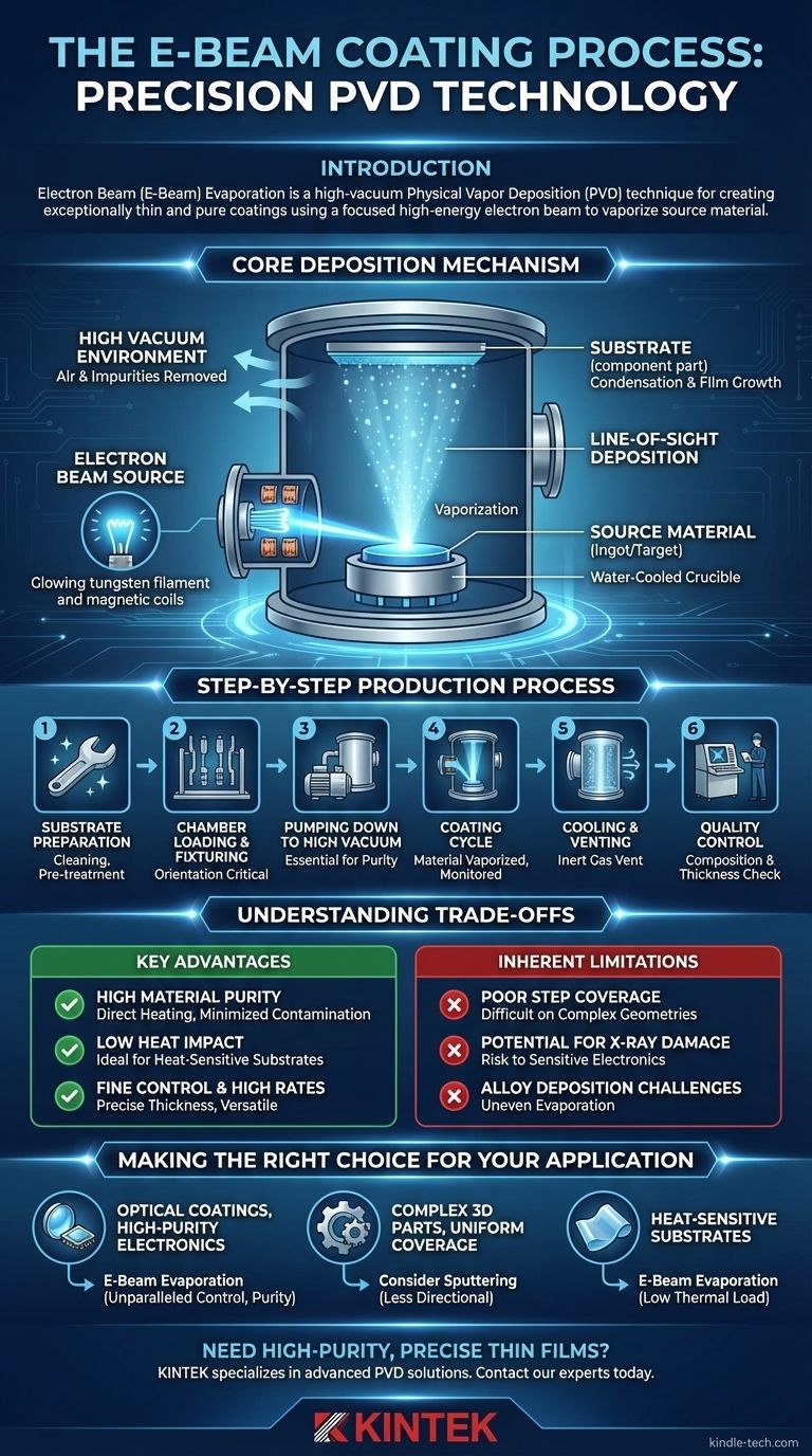
電子ビーム(E-beam)蒸着は、極めて薄く純粋なコーティングを作成するために使用される高真空物理気相成長(PVD)技術です。このプロセスでは、集束された高エネルギーの電子ビームを使用して原料を加熱し、蒸発させます。この蒸気が直進し、基板上に凝縮して、原子レベルで精密な膜を形成します。
Eビームコーティングは、本質的に直進性の成膜プロセスであり、その精度とコーティング対象部品への熱的影響が少ないことで高く評価されています。特に純度の高い高密度膜の作成に優れていますが、その指向性のため、複雑な三次元形状のコーティングには課題があります。
コアとなる成膜メカニズム
Eビームプロセスを理解するには、真空チャンバー内で起こる基本的な物理現象を把握することが不可欠です。各ステップは、特定の膜組成と厚さを達成するために精密に制御されます。
真空環境
プロセス全体は高真空チャンバー内で行われます。チャンバーの排気は、蒸発した材料と反応して最終膜を汚染する可能性のある空気やその他のガス状の不純物を除去するために極めて重要です。このほぼ真空の状態により、蒸気原子は他の粒子と衝突することなく基板に直接到達できます。
電子ビーム源
タングステンフィラメントが加熱され、電子の流れが生成されます。これらの電子は、ブラウン管(CRT)テレビが機能するのと同様に、一連の磁場を使用して加速され、高エネルギービームに集束されます。
原料の蒸発
この集束された電子ビームは、水冷式の銅製るつぼに保持されている原料(インゴットまたはターゲットと呼ばれることが多い)に向けられます。ビームからの強烈なエネルギーにより、材料は沸点まで加熱され、蒸発または昇華して蒸気になります。
直進性の成膜(Line-of-Sight Deposition)
蒸気原子は、源から基板へ直線的かつ直接的な経路で移動します。この「直進性」特性は、コーティングが蒸発源から直接見える表面にのみ堆積することを意味します。
凝縮と膜の成長
蒸気原子が比較的冷たい基板表面に到達すると、凝縮します。このプロセスにより、原子レベルで層を重ねてコーティングが形成され、非常に微細で高密度の薄膜が得られます。
段階的な製造プロセス
コアメカニズムから産業用途への移行には、注意深く管理された一連の製造ステップが含まれます。
ステップ 1: 基板の準備
清浄な表面がなければ、適切な密着は不可能です。このステップでは、汚染物質を除去するための厳格な洗浄が行われます。部品の履歴に応じて、古いコーティングの剥離や、表面を準備するための特定の予備処理が含まれる場合もあります。
ステップ 2: チャンバーへの装填と固定
原料はるつぼにセットされ、基板は専用の治具またはホルダーに取り付けられます。このプロセスの直進性の性質上、これらの治具の向きは、ターゲット表面が蒸気流に正しくさらされるようにするために重要です。
ステップ 3: 高真空への排気
装填後、チャンバーは密閉され、目標圧力レベルまで排気されます。この排気にはかなりの時間がかかることがありますが、最終的なコーティングの純度には不可欠です。
ステップ 4: コーティングサイクル
真空が確立されると、電子ビームが作動し、材料が蒸発します。膜が正確な仕様を満たしていることを確認するために、成膜速度と最終膜厚がリアルタイムで監視されます。材料と必要な厚さに応じて、サイクル全体は30分から数時間に及ぶことがあります。
ステップ 5: 冷却とベント(大気圧に戻す)
目標の厚さに達した後、電子ビームは停止されます。チャンバーを不活性ガスでパージして大気圧に戻す前に、システムを冷却させます。
ステップ 6: 品質管理
各バッチは厳格な検査を受けます。技術者は、X線蛍光(XRF)装置などのツールを使用してコーティングの組成と厚さを検証し、すべての要件を満たしていることを確認します。
トレードオフの理解
単一のコーティング技術がすべての用途に完璧であるわけではありません。Eビーム蒸着には、その理想的な使用例を定義する明確な利点と限界があります。
主な利点
- 高い材料純度: 電子ビームは原料のみを直接加熱し、るつぼ全体を加熱しないため、汚染が最小限に抑えられ、極めて純粋な膜が得られます。
- 低い熱影響: このプロセスは、他の方法と比較して基板への熱伝達が少ないため、プラスチック、ポリマー、または組み立て済みの電子部品などの熱に敏感な材料のコーティングに最適です。
- 精密な制御と高いレート: 成膜速度と膜厚を非常に精密に制御できると同時に、金属やセラミックを含む幅広い材料に対して非常に高い蒸発速度を達成できます。
固有の限界
- ステップカバレッジの悪さ: 非常に指向性の高い蒸気流のため、複雑な形状、鋭いエッジ、または内部表面を均一にコーティングすることは困難です。主に「見える」部分のみをコーティングします。
- X線による損傷の可能性: 高エネルギー電子が原料と相互作用することでX線が発生する可能性があります。通常は低レベルですが、これらは非常に敏感な電子基板や光学部品に損傷を与えるのに十分な場合があります。
- 合金成膜の難しさ: 蒸気圧の異なる複数の元素(合金)からなる材料を蒸発させるのは難しい場合があります。なぜなら、より揮発性の高い元素が先に蒸発してしまうからです。
用途に応じた適切な選択
正しいPVD法を選択するには、プロセスの能力と主要なエンジニアリング目標を一致させる必要があります。
- 光学コーティングまたは高純度エレクトロニクスが主な焦点の場合: Eビーム蒸着は、膜の厚さ、純度、密度に関して比類のない制御を提供し、これらの用途には極めて重要です。
- 複雑な3D部品を均一なカバレッジでコーティングすることが主な焦点の場合: スパッタリングのような、より指向性の低いPVD法を検討する必要があります。これにより、すべての表面が適切にコーティングされることが保証されます。
- 熱に敏感な基板のコーティングが主な焦点の場合: Eビームプロセスの低い熱負荷は、ポリマーやデリケートな組み立て済み部品などの材料を保護するための優れた選択肢となります。
結局のところ、Eビーム蒸着の選択は、幾何学的な均一なカバレッジの達成よりも最終的な膜の品質と精度がより重要となる用途のための戦略的な決定となります。
要約表:
| 主要な側面 | 詳細 |
|---|---|
| プロセスタイプ | 物理気相成長(PVD) |
| 環境 | 高真空 |
| メカニズム | 直進性成膜 |
| 主な利点 | 高純度、低い熱影響、精密な厚さ制御 |
| 理想的な用途 | 光学コーティング、高純度エレクトロニクス、熱に敏感な基板 |
| 限界 | 複雑な3D形状に対するカバレッジの悪さ |
研究や製造のために高純度で精密な薄膜が必要ですか?
KINTEKは、要求の厳しい用途向けのPVDソリューションを含む高度なラボ機器を専門としています。当社の専門知識は、特定の基板と目標に対して優れた膜品質、純度、性能を保証するために、適切なコーティング技術を選択するのに役立ちます。
当社の専門家に今すぐお問い合わせいただき、薄膜成膜のニーズにおいて当社がどのように研究室をサポートできるかをご相談ください。
ビジュアルガイド
関連製品
- 高温用途向け電子ビーム蒸着コーティングタングステンるつぼおよびモリブデンるつぼ
- 電子ビーム蒸着コーティング用導電性窒化ホウ素るつぼ BNるつぼ
- 蒸着用電子ビーム蒸着コーティング金めっきタングステンモリブデンるつぼ
- 電子ビーム蒸着コーティング 無酸素銅るつぼおよび蒸着用ボート
- 電子ビーム蒸着用高純度純グラファイトるつぼ


