「薄膜の範囲」と言うとき、我々が指しているのは単一の指標ではなく、この技術が持つ4つの主要な側面における広大な範囲です。その物理的な厚さは、通常、数ナノメートルから数マイクロメートルに及びます。さらに重要なのは、その範囲が膨大な種類の材料、幅広い機能特性、そしてマイクロチップから医療機器に至るまで、絶えず拡大しているハイテク応用のリストを含むということです。
薄膜技術の核となる概念は、その物理的な寸法だけではなく、多用途なプラットフォームとしての機能にあります。ナノスケールで材料層を精密に制御することにより、バルク材料では達成不可能な独自の光学特性、電気特性、機械的特性を設計することができます。
定義される「範囲」:膜厚
「範囲」の最も文字通りの解釈は厚さです。この次元が、他のすべての特性が生まれる基礎となります。
単原子層からマイクロメートルまで
薄膜とは、その厚さが単一原子層(1ナノメートルの分数)から数マイクロメートル(µm)に及ぶ材料の層のことです。
ほとんどの産業用途は、10ナノメートルから10マイクロメートルの範囲で稼働します。このスケールは、材料がユニークな特性を示すのに十分薄く、かつ堅牢で機能的であるのに十分な厚さであるというスイートスポットです。
厚さが重要である理由
これらの微小な寸法では、バルク材料では無視できる効果が支配的になります。これには、量子力学的現象、光学的干渉、および独自の応力-ひずみ関係が含まれ、エンジニアは単に厚さを調整するだけで材料の性能を微調整することができます。
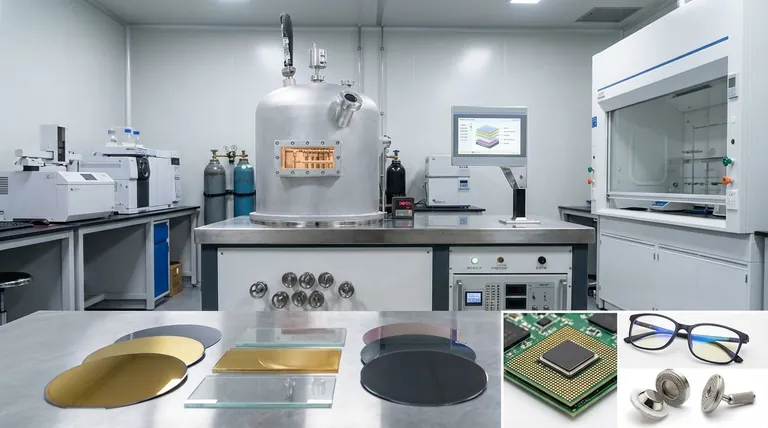
材料とプロセスの範囲
薄膜技術の多様性は、堆積させることができる材料の広範な配列と、それを行うために使用される方法の精度に直接関連しています。
金属から先進セラミックスまで
事実上あらゆる種類の材料を薄膜にすることができます。参照資料では、以下を含む幅広い選択肢が強調されています。
- 金属:アルミニウム、高融点金属
- 誘電体・セラミックス:酸化ケイ素、窒化物(TiN)
- 半導体:シリコン、ゲルマニウム、化合物半導体(GaAs)
- 特殊材料:ダイヤモンドライクカーボン(DLC)、および新興のアモルファス酸化物
この材料の多様性により、ほぼすべての工学的課題に合わせて調整されたコーティングを作成することが可能になります。
精度を可能にするプロセス
これらの膜を作成するには、高度に制御された環境と洗練された装置が必要です。主要な方法には以下が含まれます。
- 化学気相成長法(CVD):前駆体ガスを使用して表面上に膜を「成長」させ、均一で高純度の層を作成するのに理想的です。
- 物理気相成長法(PVD):真空中で固体材料を蒸発させ(スパッタリングまたは蒸着)、基板上に凝縮させるもので、金属や硬質コーティングに優れています。
- イオン注入:荷電原子(イオン)を表面に注入し、その化学的および物理的特性を変化させます。
達成可能な特性のスペクトル
材料を薄膜として堆積させるのは、バルク材料とは異なる特定の機能特性を達成するためです。
光学特性の操作
薄膜は光を制御するために不可欠です。ディスプレイ向けに高度に透明に、レンズ向けに反射防止に、または鏡向けに高反射率になるように設計できます。
電気的挙動の制御
膜の電気特性は正確に調整できます。これらは、マイクロチップ配線の導体、コンデンサの絶縁体(誘電体)、またはトランジスタの半導体として機能します。
機械的耐久性の向上
薄膜は保護コーティングとして使用されることがよくあります。窒化チタン(TiN)やダイヤモンドライクカーボン(DLC)などの材料は、切削工具や摺動部品向けに超硬質で耐擦傷性があり、低摩擦の表面を作り出します。
現代の応用の広がり
材料と特性の組み合わせにより、薄膜は現代の技術を定義する非常に幅広い用途を持っています。
- 半導体製造:シリコンウェーハ上のトランジスタ、配線、絶縁体を形成し、あらゆる集積回路の基礎をなします。
- ディスプレイ・光学:液晶テレビやスマートフォン画面から、コーティングされた眼鏡や高性能レンズに至るまで、あらゆるものを可能にします。
- データストレージ:ハードディスクの磁気層や光ディスクの相変化層の作成に使用されます。
- 医療機器:インプラント用の生体適合性コーティングや、手術器具用の耐久性のある滅菌表面を提供します。
内在するトレードオフの理解
薄膜技術は強力ですが、課題や限界がないわけではありません。これらを理解することが、その成功裏の応用にとって重要です。
コストと複雑さ
CVDやPVDなどの堆積プロセスの装置は高価であり、操作と保守にはかなりの専門知識が必要です。これにより、製造への参入障壁が高くなります。
基板への依存性
薄膜は基板(シリコンウェーハやガラス片など)上に堆積させる必要があります。膜の密着性、応力、最終的な特性は、この基板の選択とその表面処理に大きく依存します。
耐久性と安定性
極めて薄い層は壊れやすく、傷、剥離、または環境劣化の影響を受けやすい場合があります。望ましい特性(透明性など)を達成するには、長期的な耐久性とのトレードオフが伴うことがよくあります。
目的別に「範囲」を捉える方法
薄膜技術の「範囲」は、特定の目的のレンズを通して理解するのが最適です。
- 材料科学またはR&Dに主な焦点を当てる場合:透明トランジスタ向けのアモルファス酸化物のような新しい材料の組み合わせの範囲が、イノベーションにとって最も重要な分野です。
- 製造とエンジニアリングに主な焦点を当てる場合:堆積プロセス(CVD、PVD)の範囲と、それらを制御して一貫した膜特性を実現する能力が、主要な変数となります。
- 製品開発に主な焦点を当てる場合:光学からエレクトロニクスなどにわたる応用の範囲が、この技術が競争優位性を提供できる市場機会を定義します。
結局のところ、薄膜は、微視的なスケールで物質を工学的に設計する力を私たちに与える基礎的な技術なのです。
要約表:
| 範囲の側面 | 主要な詳細 |
|---|---|
| 厚さ | 単原子層(<1 nm)から数マイクロメートル(µm) |
| 材料 | 金属(Al、Ti)、セラミックス(TiN)、半導体(Si、GaAs)、DLC |
| 主要特性 | 光学(透明度)、電気(導電性)、機械的(硬度) |
| 主な応用 | 半導体、ディスプレイ、データストレージ、医療機器 |
精密な薄膜で優れた表面のエンジニアリングを始める準備はできていますか? KINTEKは、薄膜堆積(CVD、PVD)および分析のための高度なラボ装置と消耗品を専門としています。R&Dであれ製造であれ、当社のソリューションは、一貫した高性能コーティングの実現を支援します。お客様固有のラボのニーズをサポートし、イノベーションを加速する方法について、今すぐ専門家にご相談ください。
ビジュアルガイド

関連製品
- 薄膜成膜用アルミニウムコーティングセラミック蒸着用ボート
- 薄膜成膜用タングステン蒸着用ボート
- 電子ビーム蒸着コーティング 無酸素銅るつぼおよび蒸着用ボート
- 高温用途向けモリブデン・タングステン・タンタル蒸着用ボート
- リチウム電池包装用アルミニウム・プラスチック複合フィルム


